Purpose
The RT8071C is a high efficiency synchronous, step-down DC/DC converter. Its input voltage ranges from 2.7V to 5.5V that provides an adjustable regulated output voltage from 0.6V to VIN while delivering up to 3A of output current. This document explains the function and use of the RT8071C evaluation board (EVB), and provides information to enable operation, modification of the evaluation board and circuit to suit individual requirements.
Introduction
General Product Information
The RT8071C is a high efficiency synchronous, step-down DC/DC converter. Its input voltage ranges from 2.7V to 5.5V that provides an adjustable regulated output voltage from 0.6V to VIN while delivering up to 3A of output current. The internal synchronous low On-resistance power switches increase efficiency and eliminate the need for an external Schottky diode. The switching frequency is fixed internally at 1MHz. The 100% duty cycle provides low dropout operation, hence extending battery life in portable systems. Current mode operation with internal compensation allows the transient response to be optimized over a wide range of loads and output capacitors. The RT8071C is available in a WDFN-10L 3x3 package.
Product Feature
-
High Efficiency : Up to 95%
-
Low RDS(ON) Power Switches : 69mΩ/49mΩ
-
Current Mode Operation
-
Fast Transient Response
-
Fixed Frequency : 1MHz
-
No Schottky Diode Required
-
Internal Compensation
-
0.6V Reference Allows Low Output Voltage
-
Low Dropout Operation : 100% Duty Cycle
-
OCP, UVP, OTP
-
OpenVReg Type 0-LV Compliant
Key Performance Summary Table
|
Key Features
|
Evaluation Board Number : PCB052_V1
|
|
Input Voltage Range
|
2.7V to 5.5V
|
|
Max Output Current
|
3A
|
|
Default Output Voltage
|
1.05V
|
|
Default Marking & Package Type
|
RT8071CGQW, WDFN-10L 3x3
|
|
Operation Frequency
|
Steady 1MHz at all loads
|
Bench Test Setup Conditions
Headers Description and Placement
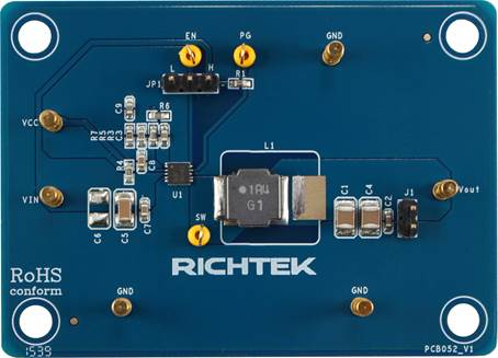
Please carefully inspect the EVB IC and external components, comparing them to the following Bill of Materials, to ensure that all components are installed and undamaged. If any components are missing or damaged during transportation, please contact the distributor or send e-mail to evb_service@richtek.com
Test Points
The EVB is provided with the test points and pin names listed in the table below.
|
Test point/
Pin name
|
Signal
|
Comment (expected waveforms or voltage levels on test points)
|
|
FB
|
Feedback voltage input
|
Feedback Input. This pin receives the feedback voltage from a resistive voltage divider connected across the output.
|
|
VCC
|
Supply voltage input.
|
Supply Voltage Input. Decouple this pin to GND with at least 1µF ceramic capacitor.
|
|
VIN
|
Input voltage
|
Power input. Support 2.7V to 5.5V Input Voltage. Decouple this pin to GND with at least 10µF ceramic capacitor.
|
|
GND
|
Ground
|
Ground. The exposed pad must be soldered to a large PCB and connected to GND for maximum power dissipation.
|
|
SW
|
Switch node test point
|
Switch Node. Connect this pin to the inductor.
|
|
NC
|
No connection
|
No Internal Connection.
|
|
PGOOD
|
Power good indicator
|
Power Good Indicator. This pin is an open drain logic output. The PGOOD will be pulled to ground when the output voltage is less than 90% of the target output voltage.
|
|
EN
|
Enable test point
|
Enable Control Input. Pull high the EN pin to turn on the converter.
|
Power-up & Measurement Procedure
1. Connect input power (2.7V < VIN < 5.5V) and input ground to VIN and GND test pins respectively.
2. Connect positive end and negative terminals of load to VOUT and GND test pins respectively.
3. There is a 3-pin header “EN” for enable control. To use a jumper at “H” option to tie EN test pin to input power VIN for enabling the device. Inversely, to use a jumper at “L” option to tie EN test pin and ground GND for disabling the device.
4. Verify the output voltage (approximately 1.05V) between VOUT and GND.
5. Connect an external load up to 3A to the VOUT and GND terminals and verify the output voltage and current.
Output Voltage Setting
Set the output voltage with the resistive divider (R3, R5) between VOUT and GND with the midpoint connected to FB. The output is set by the following formula :
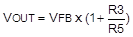
Schematic, Bill of Materials & Board Layout
EVB Schematic Diagram
Bill of Materials
|
Reference
|
Qty
|
Part Number
|
Description
|
Package
|
Manufacture
|
|
U1
|
1
|
RT8071CGQW
|
DC/DC Converter
|
WDFN-10L 3x3
|
RichTek
|
|
C1, C4
|
2
|
C3225X5R0J226M
|
22µF/25V/X5R
|
1210
|
TDK
|
|
C5
|
1
|
C3225X5R0J106M
|
10µF/50V/X5R
|
1210
|
TDK
|
|
C6
|
1
|
|
NC
|
1210
|
TDK
|
|
C3, C9
|
1
|
0603B681K500NT
|
680pF/50V/X7R
|
0603
|
WALSIN
|
|
C2, C7, C8
|
3
|
0603B104K500NT
|
0.1µF/50V/X7R
|
0603
|
WALSIN
|
|
EC1
|
1
|
|
NC
|
1206
|
JACKSON
|
|
L1
|
1
|
NR8040T1R4N
|
1.4µH
|
|
TAIYO
|
|
R1
|
1
|
WR06X1003FT
|
100k
|
0603
|
WALSIN
|
|
R3
|
1
|
WR06X6201FT
|
6.2k
|
0603
|
WALSIN
|
|
R5
|
1
|
WR06X8201FT
|
8.2k
|
0603
|
WALSIN
|
|
R4, R6
|
2
|
WR06X000PT
|
0
|
0603
|
WALSIN
|
|
R7
|
1
|
WR06X1802FT
|
18k
|
0603
|
WALSIN
|
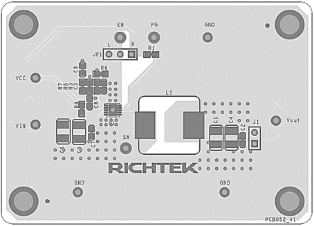
PCB Layout
Top View
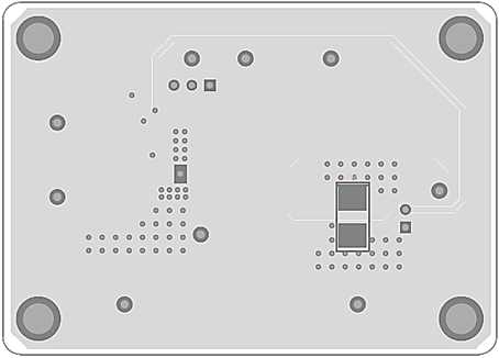
Bottom View